AndrewBurns
Member
A truly spectacular achievement and great photo looking! A 350W UV LED, wow...
I've done a little work related to DLP UV projection, so I'm curious about that have you tested the cyanotype process for different wavelengths like 405 nm? Increasing the UV wavelength from 365-385 nm to 405 nm means that many devices designed for visible light can operate much better, and sometimes the increased transmission efficiency can compensate for the decrease in photon energy. This article here suggests that the exposure efficiency of 405nm is about half that of 365nm: https://pubs.rsc.org/en/content/getauthorversionpdf/C4PP00166D
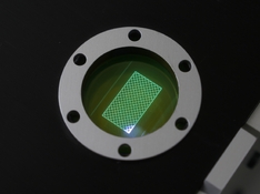
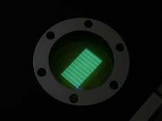
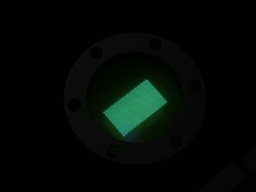
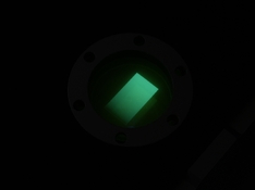
Thanks! Yes previously I've used a 405nm UV source and an LCD screen for contact printing (placing the LCD screen directly onto the paper and shining UV light through the screen to form the exposure) and it worked perfectly fine for cyanotype. I was able to get very short exposure times with this system, however it was limited to the size of the LCD screen which is why I decided to make the projector.
You're right that shorter wavelengths are less optically efficient, both in that lenses and the LCD screen absorb it more strongly and also the LEDs themselves are less efficient, and so although the process might have a peak sensitivity at a short wavelength you might get your best exposure time at a longer wavelength. The reason I dropped from 405 to 380nm for my projector is because I wanted to expose gelatine sensitised with DAS which barely responds at all to 405nm but is reasonably sensitive to 380nm. Although I've recently found that even with the shorter wavelength I'm struggling to get a good exposure because DAS has a minimum amount of energy required to activate and my projector is struggling to generate that much energy despite how powerful it is.